Something unusual is happening in Indian engineering hiring: companies are recruiting for factories that are not finished yet. India's semiconductor push has moved from announcements to concrete plants — assembly and test facilities in Gujarat are operational, and Tata Electronics' wafer fab at Dholera is targeting first production around the end of 2026 — and the hiring is running ahead of the concrete.
For a country whose engineering graduates have spent two decades defaulting to IT services and software, that is a genuinely new option. This guide covers what semiconductor and VLSI careers in India actually involve, the roles that exist, which skills are being asked for, and how to break in — whether you are a fresher choosing a direction or an engineer considering a switch.
What actually changed
For years "India will make chips" was a press release. The shift is that several projects are now physically running or under construction under the India Semiconductor Mission, with committed investment reported in the range of ₹1.5 lakh crore and above across participants including Tata Electronics, Micron, CG Power, Kaynes and others.
Two distinctions worth understanding before you plan a career around it, because job adverts blur them:
- Fabrication (front-end) — actually making the wafer. Extremely capital-intensive, and the part India is only now starting, with Tata's Dholera fab targeting mature nodes rather than leading-edge.
- ATMP / OSAT (back-end) — assembly, testing, marking and packaging. Cheaper to build, faster to bring online, and where most of India's operational capacity is today.
- Design — the part India has quietly been strong at for twenty-five years. Qualcomm, Intel, AMD, Nvidia, Texas Instruments, Synopsys, Cadence and Broadcom have run large India design centres for a long time, and a very significant share of global chip design work already happens in Bengaluru, Hyderabad, Noida and Pune.
That third point matters more than the headlines suggest: if you want to work on chips in India, design has been hiring all along. The new fabs add manufacturing careers that essentially did not exist domestically, but they do not replace the design route — which remains the larger and more accessible entry path.
The roles, honestly described
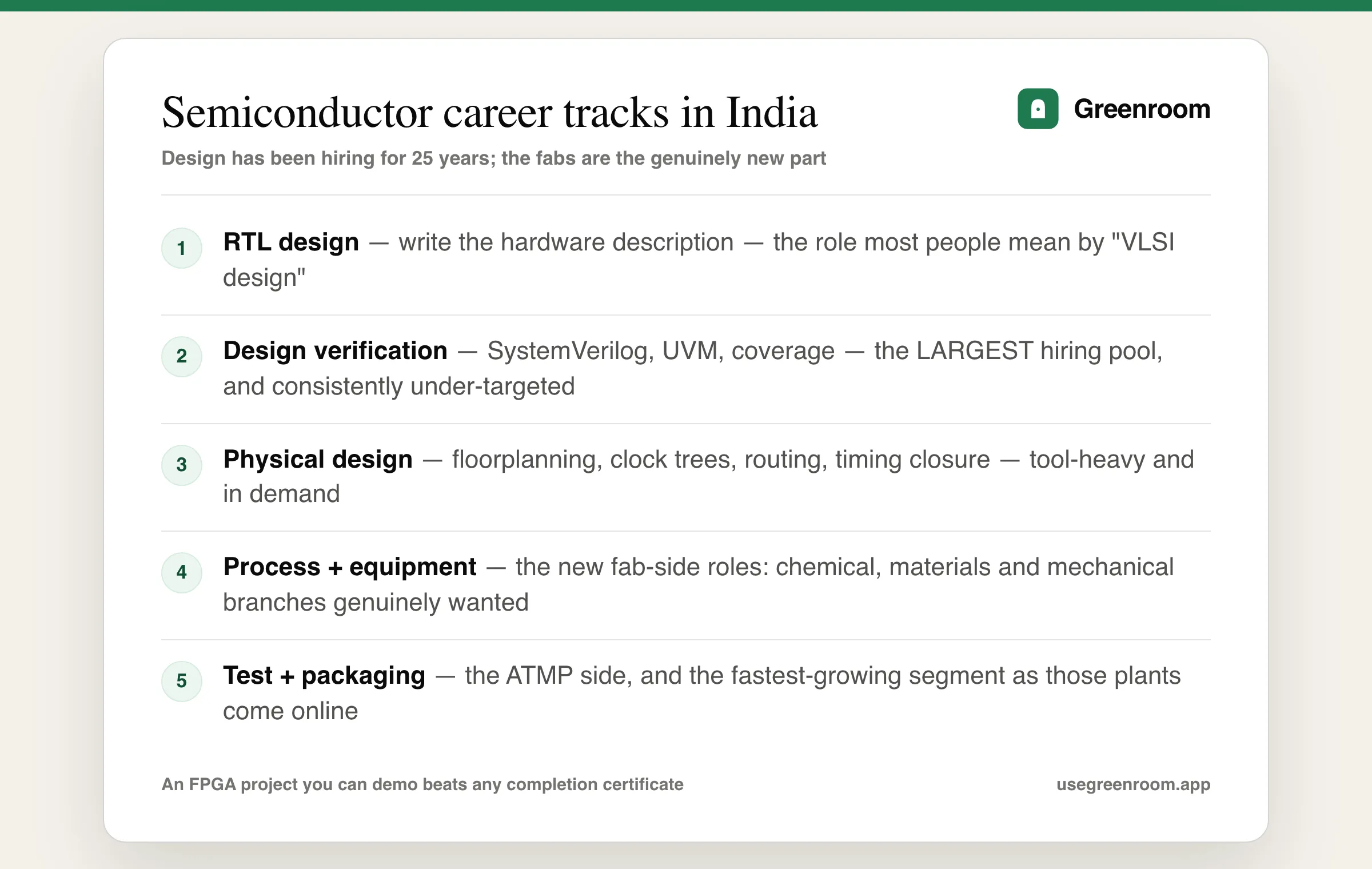
- RTL design engineer — write the hardware description (Verilog/SystemVerilog, VHDL) that defines what the circuit does. Highly sought, and the role most people mean by "VLSI design".
- Design verification (DV) engineer — prove the design does what it should, using SystemVerilog and UVM, constrained-random stimulus and coverage. This is where the largest share of hiring sits, because verification typically consumes more effort than design itself. It is also the most realistic entry point for a strong software-leaning graduate, and candidates consistently under-target it.
- Physical design engineer — take the synthesised design to a manufacturable layout: floorplanning, placement, clock tree synthesis, routing, timing closure. Tool-heavy (Synopsys, Cadence) and in demand.
- Analog / mixed-signal design — the specialism with the deepest theory requirement and the longest ramp; usually needs a relevant master's.
- DFT engineer — design for testability, scan chains, built-in self-test. Unfashionable and consistently short of people.
- Embedded / firmware — the software layer next to the silicon. The easiest crossover for a software engineer.
- Process / equipment / cleanroom engineer — the genuinely new fab-side roles. Chemical, materials, mechanical and industrial engineering backgrounds matter here far more than CS, which is worth saying because non-CS branches are usually told their degree is a disadvantage in tech hiring.
- Test and packaging engineer — the ATMP side, and the fastest-growing segment as those plants come online.
Industry commentary projects large workforce growth over the next few years, with talent-tracking studies putting India's current chip workforce in the low hundreds of thousands and projecting substantially higher demand. Treat specific headcount projections as directional rather than precise — they are estimates from interested parties — but the direction is consistently reported the same way, and the current shortfall in fab-ready, packaging and test-engineering talent is widely acknowledged.
What to actually learn
For the design and verification track, which is the realistic route for most readers:
- Digital electronics fundamentals — combinational and sequential logic, FSMs, setup and hold time, metastability, clock domain crossing. These are the interview questions, essentially without exception.
- Verilog / SystemVerilog — non-negotiable. Write it, simulate it, and be able to explain the difference between blocking and non-blocking assignments without hesitating, because you will be asked.
- Computer architecture — pipelining, hazards, caches, memory hierarchy.
- For DV specifically: UVM, constrained-random verification, functional coverage, assertions. Plus scripting — Python, Perl or Tcl — because verification engineers automate constantly.
- For physical design: static timing analysis, and familiarity with the standard toolchains.
- Protocols — AMBA (AXI, AHB, APB), and at least one of PCIe, DDR or USB. Naming a protocol you have actually worked with is a strong differentiator.
For the fab / manufacturing track: semiconductor process fundamentals (lithography, etching, deposition, ion implantation), cleanroom protocol, statistical process control and yield analysis, and equipment handling. Chemical, materials and mechanical engineers are genuinely wanted here.
Two credentials worth knowing about: several institutes and government-backed programmes offer VLSI and semiconductor training with tool access, and a project on an FPGA board is worth more than any certificate. An FPGA project you can demo and explain beats a course completion certificate every time — it demonstrates you have debugged real timing, not watched a video.
What the interviews are like
Different from a software loop in a way worth preparing for. Reported patterns:
- Fundamentals are examined properly. Expect to be asked to draw a circuit on a whiteboard, work through setup/hold violations, or explain metastability and synchronisers. There is much less tolerance for "I'd look it up" than in software interviews.
- Puzzles and digital design problems — design a counter with constraints, a FIFO, a clock divider by an odd number, an arbiter.
- Code reading, not just writing. You may be given Verilog and asked what it synthesises to, or what is wrong with it.
- Project depth — whatever you built, expect to be pushed on why, what broke, and what you would change. Our how to explain your project guide covers the structure.
- Less DSA — some companies include coding rounds, but LeetCode-grinding is a much smaller factor here than in product-company software hiring.
Our embedded systems interview questions guide covers the nearest adjacent syllabus, and the computer networks and operating systems guides cover fundamentals that appear in firmware-leaning loops.
Should you switch? An honest weighing
Reasons it is genuinely attractive: the domain is expanding rather than contracting; expertise compounds and is hard to automate away, which is a real contrast with the current anxiety in generalist software hiring; senior specialists in verification and physical design are scarce and paid accordingly; and non-CS engineering branches are actually wanted, which is rare.
Reasons to be careful, stated plainly:
- The ramp is long. Meaningful competence in VLSI takes years, not a three-month bootcamp. This is a career decision, not a pivot you undo in six months.
- Entry salaries are often below equivalent software roles, with the curve crossing later as specialisation compounds. Go in knowing that.
- Manufacturing roles mean plant locations — Sanand, Dholera, and similar — not necessarily Bengaluru or your home city. Shift work is normal in fabs.
- Projects are long and capital-intensive, and timelines can slip. Build your plan around the design ecosystem that already exists rather than around a single announced plant.
- Fewer switch-back options. Moving from software to VLSI is easier than the reverse.
The balanced read: if you are an electronics, electrical, instrumentation or similar branch student who has been told your degree is a disadvantage, this is the most credible counter-argument in years. If you are a CS graduate already doing well in software, the case is weaker unless you are specifically drawn to the domain — and "the industry is growing" is not, by itself, a reason to spend three years learning something you find dull.
NPTEL, tool licences, ChatGPT — where each fits
- NPTEL and institute courses on digital design and VLSI — free, rigorous, and taught by people who examine this material.
- An FPGA board — the single highest-return purchase in this field. Cheap boards are enough to build, simulate and debug something real.
- Open-source toolchains — Verilator, Icarus Verilog, GTKWave, and the open silicon toolchains let you practise without commercial licences.
- Government-backed and institute VLSI programmes — worth checking specifically because some offer access to commercial tools, which is otherwise the hardest thing to get.
- Company career pages over job boards — semiconductor hiring is less aggregated than software; check design-centre pages directly.
- ChatGPT — useful for explaining concepts and reviewing HDL. It cannot substitute for having debugged a timing violation yourself, which is what the interview probes.
- Greenroom — the spoken layer. Ari, the AI interviewer, rehearses the project deep-dive and fundamentals questions out loud, which is the part of a hardware loop candidates prepare least. Fair tradeoff: Ari does not teach VLSI — pair it with the coursework.
A practical entry plan
- Months 1–2: digital electronics fundamentals until setup/hold, metastability and CDC are reflexive. Verilog daily.
- Months 3–4: build something on an FPGA — a UART, a FIFO, a simple processor. Debug it properly; the debugging is the learning.
- Months 5–6: specialise. SystemVerilog and UVM if targeting verification (the largest hiring pool), or STA and the physical-design flow if targeting backend.
- Throughout: one protocol in depth, scripting in Python, and rehearse your project explanation out loud until it is two crisp minutes.
Also useful: our embedded systems guide, the campus placement guide for the drive process, and the service to product switch guide for the transition mechanics if you are moving from IT services.
Frequently asked questions
Is semiconductor a good career option in India in 2026?
It is a genuine and expanding option, with the important nuance that India's chip design ecosystem has been hiring for over two decades through the India centres of Qualcomm, Intel, AMD, Nvidia, Texas Instruments and the EDA vendors, while manufacturing is the genuinely new part. The domain rewards deep expertise that compounds over time, but the ramp is measured in years rather than months and entry salaries are often below equivalent software roles.
What is the difference between VLSI design, verification and physical design?
RTL design engineers write the hardware description that defines circuit behaviour, usually in Verilog or SystemVerilog. Design verification engineers prove the design behaves correctly using SystemVerilog, UVM, constrained-random stimulus and coverage, and this is where the largest share of hiring sits because verification consumes more effort than design. Physical design engineers turn the synthesised design into a manufacturable layout through floorplanning, placement, clock tree synthesis, routing and timing closure.
Which skills do semiconductor companies in India hire for?
For design and verification tracks: digital electronics fundamentals including setup and hold time, metastability and clock domain crossing; Verilog and SystemVerilog; computer architecture; UVM, functional coverage and assertions for verification; static timing analysis for physical design; scripting in Python or Tcl; and familiarity with a protocol such as AMBA, PCIe or DDR. For fab roles: process fundamentals, cleanroom protocol, statistical process control and yield analysis.
Can a computer science graduate move into VLSI?
Yes, and design verification is usually the most realistic entry point because it is heavily software-shaped — SystemVerilog, UVM, constrained-random testing and scripting all reward software instincts, and it is where the largest volume of hiring sits. You will still need to build genuine digital electronics fundamentals, since interviews examine setup and hold timing, metastability and synchronisers directly rather than accepting that you would look them up.
What do semiconductor interviews in India involve?
They lean much harder on fundamentals than software interviews do. Expect whiteboard circuit questions, setup and hold violation analysis, metastability and synchroniser design, and digital design problems such as building a FIFO, an arbiter or an odd-number clock divider. You may be given Verilog to read and asked what it synthesises to or what is wrong with it. Project depth is probed thoroughly, and data structures rounds are far less central than in product-company software hiring.
Is an FPGA project better than a VLSI certification course?
Generally yes. A project you built on an FPGA board and can demo and explain demonstrates that you have debugged real timing behaviour, which is precisely what interviewers probe, whereas a completion certificate demonstrates attendance. Build something like a UART, a FIFO or a simple processor, debug it properly since the debugging is where the learning happens, and be able to explain in two minutes why you made each design decision.